● Silicon Carbide Substrate
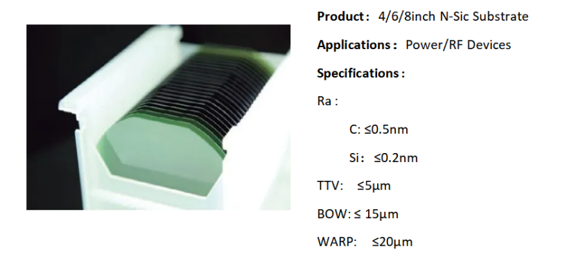
Silicon carbide (SiC) is a wide bandgap semiconductor material composed of carbon and silicon elements, known as the third-generation semiconductor material. It possesses several notable characteristics, such as a wider bandgap, higher thermal conductivity, breakdown voltage, and electron saturation drift velocity than silicon. These properties make silicon carbide highly suitable for manufacturing high-frequency, high-power devices that can withstand high temperatures, pressures, and electric currents.
Silicon carbide substrates can be categorized into conductive and semi-insulating types based on their electrical resistivity. Conductive silicon carbide substrates are primarily used for the fabrication of power semiconductor devices, while semi-insulating substrates are used for radio-frequency devices. The growth techniques for silicon carbide substrates involve epitaxial growth on silicon carbide single-crystal substrates, used for manufacturing power devices, and the growth of gallium nitride epitaxial layers on silicon carbide for high-frequency power and optoelectronic devices.
The main application fields of silicon carbide substrates include new energy vehicles, photovoltaic power generation, rail transportation, and more. Compared to traditional silicon-based power chips, silicon carbide chips offer significant advantages in the power semiconductor field, such as higher current and voltage tolerance, faster switching speeds, lower energy loss, and better high-temperature resistance. These advantages position silicon carbide as a crucial material for the future of power devices.
As an advanced semiconductor material, silicon carbide substrates hold broad application prospects, particularly demonstrating immense potential in the manufacturing of high-power and high-frequency devices.
Learn More:0086-186 8368 5911(Wechat); zhangw@timemaker.com
● Diamond Wafer
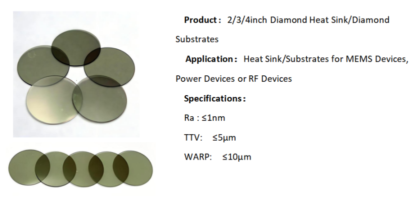
Diamond, as an ultra-wide bandgap semiconductor material, possesses unique properties that make it promising for applications in the semiconductor and integrated circuit fields. With its exceptionally high thermal conductivity, surpassing that of traditional semiconductor materials, diamond is an ideal material for heat dissipation. Its use as a heat sink in high-power semiconductor devices is garnering increasing attention. The connection technology between diamond and semiconductor devices is one of the current research focuses, and while it faces some technical challenges, it has shown promising prospects for development.
Diamond's applications in the semiconductor field also include diamond single-crystal substrates. Artificial diamonds are primarily produced using high-pressure high-temperature (HPHT) methods and chemical vapor deposition (CVD). CVD diamonds, especially those produced by microwave plasma chemical vapor deposition (MPCVD), are widely used as heat dissipation materials under high heat flux conditions due to their high purity, high thermal conductivity, and ability to form large-area films. Such applications include radar components.
The application of diamond single-crystal substrates in the semiconductor field is still under development. As an ultra-wide bandgap semiconductor, diamond offers advantages such as ultra-high carrier mobility, high thermal conductivity, low thermal expansion coefficient, and ultra-high breakdown voltage, making it an ideal material for next-generation microelectronics and photonics. However, diamond still faces challenges in practical applications, such as difficulties in growing large-area wafers and issues with doping. Despite these challenges, the application prospects for diamond in the semiconductor field remain broad through continuous technological innovation and manufacturing process improvements.
The application of diamond in the semiconductor and integrated circuit fields is gradually expanding, with its potential as a heat dissipation and substrate material already evident. It is expected to find applications in many more areas in the future.
Learn More:0086-186 8368 5911(Wechat); zhangw@timemaker.com
● Glass Wafer
Glass substrates are circular sheets made from glass materials, typically less than 1 millimeter thick and available in various sizes similar to silicon wafers, such as 6 inches, 8 inches, and 12 inches. Glass substrates are insulators and are not used directly in circuit fabrication but primarily serve as carriers for silicon wafers. In the semiconductor field, their applications are mainly focused on the manufacturing and packaging of integrated circuits and semiconductor devices, including MEMS actuators and sensors, CMOS image sensors, memory and logic circuits, radio frequency, power electronics devices, optoelectronic devices, and microfluidic devices.
The application of glass substrates in the semiconductor field is driven by their unique electrical, physical, and chemical properties. Glass, as a versatile and universal material, possesses good thermal conductivity and mechanical stability. Glass substrates find wide and diverse applications in the semiconductor industry, including wafer-level capping, 3D TGV/glass interposers, and wafer-level optical elements. The market for glass substrates in semiconductor devices is gradually growing, with significant revenue growth expected in the coming years.
With technological advancements, high-precision ultra-thin structured glass substrates have entered mass production, with tolerances below 20 micrometers. The demand for high-precision glass substrates in high-tech applications is gradually increasing, especially in areas requiring miniaturization and high-precision components.Glass substrates, as an advanced semiconductor material, have a broad application prospect, particularly in serving as carriers for silicon wafers and in the manufacturing of semiconductor devices. With continuous technological progress and growing market demand, the application of glass substrates in the semiconductor field is expected to further expand and deepen.

Learn More:0086-186 8368 5911(Wechat); zhangw@timemaker.com
● GaSb Substrates
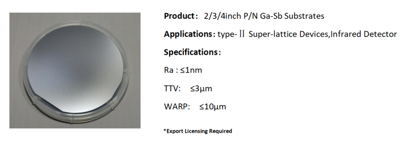
Gallium antimonide (GaSb) is a III-V group compound semiconductor material that plays a crucial role in the field of antimonide infrared optoelectronic devices due to its excellent properties. The key characteristics of GaSb substrates include a direct bandgap with a bandgap width of 0.725 eV at 300K, as well as high thermal stability. These features make GaSb an ideal material for manufacturing high-performance infrared detectors, lasers, photodetectors, and high-frequency devices, especially in the field of infrared imaging, where it excels.
The applications of GaSb substrates are extensive, covering various engineering fields from optical communications and laser technology to photosensitive detection. It is particularly suitable for fabricating devices that operate within the spectral wavelength range of 0.8μm to 4.3μm, which matches the lattice constants of several III-V compound materials, making GaSb an ideal substrate for epitaxial growth of these materials. The use of GaSb substrates can effectively reduce stress and defect issues caused by lattice mismatch, thereby enhancing device performance.
The manufacturing technologies for GaSb substrates include Liquid Encapsulated Czochralski (LEC) and Vertical Gradient Freeze (VGF) methods, which enable the growth of large-sized single crystals with low defect density and good surface quality. Additionally, the doping flexibility of GaSb substrates provides versatility in various applications, such as altering the conductivity type by doping different impurities.
In the realm of superlattice materials, GaSb is highly valued due to its unique properties. Superlattice materials are composed of semiconductor materials with two different components grown alternately in nanometer-thin layers, where GaSb exhibits outstanding performance, particularly in the field of infrared detectors. These detectors show great potential in both cooled and uncooled applications.
GaSb substrates have a wide and significant application in the semiconductor field, particularly showcasing their unique advantages in high-performance infrared optoelectronic devices and superlattice materials.
Learn More:0086-186 8368 5911(Wechat); zhangw@timemaker.com
● Germanium Wafer
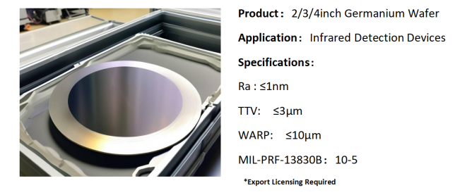
Infrared germanium substrates play a critical role in the semiconductor field and infrared optics as an important semiconductor material. The key material properties of germanium substrates include a high refractive index (approximately 4.0 in the 2-14μm wavelength band) and the optical performance changes within specific wavelength ranges. The refractive index of germanium is slightly greater than 4, which is beneficial for reducing aberrations and advantageous for optical design. Additionally, the dn/dt coefficient of germanium is relatively high, which can lead to significant focal plane displacement in infrared optical systems due to temperature changes. Germanium substrates are widely used in long-wave and mid-wave infrared optical systems, suitable for use as crown or positive elements and flint or negative elements in achromatic doublet lenses, respectively. Moreover, the transmission of germanium substrates is temperature-sensitive, so the impact of temperature changes must be considered during use.
In the semiconductor field, the applications of germanium are extensive and significant. It is used in the manufacturing of high-speed electronic and optoelectronic devices, such as high-purity germanium wafers for solar cells and infrared detectors. Germanium single crystal materials find wide applications in semiconductor device manufacturing, infrared optics, fiber optic communications, solar cells, and other fields. Germanium is chemically stable and does not react with air or water vapor at room temperature, but it can form a monolayer of GeO, which can gradually transform into a GeO2 monolayer over time. At temperatures between 600 and 700°C, GeO2 is quickly formed.
The applications of germanium substrates are not limited to the semiconductor and infrared optics fields; they also extend to aerospace measurement and control, nuclear physics detection, fiber optic communications, chemical catalysis, biomedicine, and other areas. For example, germanium-doped fibers possess excellent properties such as high capacity, low light loss, low dispersion, long transmission distances, and resistance to environmental interference, making them the only fiber that can be engineered for applications and the main component of optical communication networks. Germanium is also used in the manufacturing of GaAs/Ge solar cells, which exhibit high radiation tolerance and performance stability in space application environments. In summary, infrared germanium substrates play a crucial role in semiconductor technology and infrared optics due to their unique material properties and wide range of applications.
Learn More:0086-186 8368 5911(Wechat); zhangw@timemaker.com

